PUBLICATIONS

2017
Wang Y, Wu G, Xiang L, Xiao M, Li Z, Gao S, Chen Q, Wei X*. Single-walled carbon nanotube thermionic electron emitters with dense, efficient and reproducible electron emission. Nanoscale [Internet]. 2017;9:17814 - 17820. 访问链接Abstract
Thermionic electron emitters have recently been scaled down to the microscale using microfabrication technologies and graphene as the filament. While possessing several advantages over field emitters, graphene-based thermionic micro-emitters still exhibit low emission current density and efficiency. Here, we report nanoscale thermionic electron emitters (NTEEs) fabricated using microfabrication technologies and single-walled carbon nanotubes (SWCNTs), the thinnest conducting filament we can use. The SWCNT NTEEs exhibit an emission current density as high as 0.45 × 10⁵ A cm−2, which is superior to that of traditional thermionic emitters and five orders of magnitude higher than that of graphene-based thermionic emitters. The emission characteristics of SWCNT NTEEs are found to strongly depend on the electrical properties of the SWCNTs, with metallic SWCNT NTEEs showing a substantially lower turn-on voltage and more reproducible emission performances than those based on semiconducting SWCNTs. Our results indicate that SWCNT NTEEs are promising for electron source applications
Li X, Cheng S, Deng S, Wei X, Zhu J, Chen Q. Direct Observation of the Layer-byLayer Growth of ZnO Nanopillar by In situ High Resolution Transmission Electron Microscopy. SCIENTIFIC REPORTS [Internet]. 2017;7:40911. 访问链接Abstract
Catalyst-free methods are important for the fabrication of pure nanowires (NWs). However, the growth mechanism remains elusive due to the lack of crucial information on the growth dynamics at atomic level. Here, the noncatalytic growth process of ZnO NWs is studied through in situ high resolution transmission electron microscopy. We observe the layer-by-layer growth of ZnO nanopillars along the polar [0001] direction under electron beam irradiation, while no growth is observed along the radial directions, indicating an anisotropic growth mechanism. The source atoms are mainly from the electron beam induced damage of the sample and the growth is assisted by subsequent absorption and then diffusion of atoms along the side surface to the top (0002) surface. The different binding energy on different ZnO surface is the main origin for the anisotropic growth. Additionally, the coalescence of ZnO nanocrystals related to the nucleation stage is uncovered to realize through the rotational motions and recrystallization. Our in situ results provide atomic-level detailed information about the dynamic growth and coalescence processes in the noncatalytic synthesis of ZnO NW and are helpful for understanding the vapor-solid mechanism of catalyst-free NW growth.
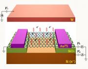
Wei X, Chen Q, Peng L-M. Thermionic electron emission from single carbon nanostructures and its applications in vacuum nanoelectronics. MRS Bulletin [Internet]. 2017;42(7):493-499 . 访问链接Abstract
Nanoscale electron sources with high electron-emitting performance are of great interest in vacuum nanoelectronics. Resembling traditional thermionic emission sources based on a hot tungsten filament, a hot carbon nanotube or graphene can function as a nanoscale electron source because of its excellent thermal stability and electrical conductivity. In this article, studies of thermionic emission from single hot carbon nanostructures are overviewed, emphasizing their differences in physics from macroscopic thermionic emission as well as potential applications in vacuum nanoelectronics. Due to their low dimensionality, nanoscale size, and nonequilibrium electron distribution, Richardson’s Law, which governs thermionic emission from macroscopic metals, breaks down in the case of thermionic emission from single carbon nanostructures, and an internal electric field in a carbon nanostructure can contribute directly to its thermionic emission. Graphene-based nanoscale thermionic emission sources, source arrays, and vacuum transistors have been fabricated and demonstrated to exhibit the advantages compared to those based on field emission. The advances imply the promise of realizing high-performance nanoscale electron sources and vacuum electronic devices based on thermionic emission.
Li H, Wang J, Gao S, Chen Q, Peng LM, Liu K, Wei X. Superlubricity between MoS2 Monolayers. Advanced Materials [Internet]. 2017;29(27):1701474 . 访问链接Abstract
The ultralow friction between atomic layers of hexagonal MoS2, an important solid lubricant and additive of lubricating oil, is thought to be responsible for its excellent lubricating performances. However, the quantitative frictional properties between MoS2 atomic layers have not been directly tested in experiments due to the lack of conventional tools to characterize the frictional properties between 2D atomic layers. Herein, a versatile method for studying the frictional properties between atomic-layered materials is developed by combining the in situ scanning electron microscope technique with a Si nanowire force sensor, and the friction tests on the sliding between atomic-layered materials down to monolayers are reported. The friction tests on the sliding between incommensurate MoS2 monolayers give a friction coefficient of ≈10−4 in the regime of superlubricity. The results provide the first direct experimental evidence for superlubricity between MoS2 atomic layers and open a new route to investigate frictional properties of broad 2D materials.
2016
Wu G, Wei X, Gao S, Chen Q, Peng LM. Tunable graphene micro-emitters with fast temporal response and controllable electron emission. NATURE COMMUNICATIONS. 2016;7. SCI被引用次数:40.
Li X, Xiao D, Zheng H, Wei X, Wang X, Gu L, Hu Y-S, Yang T, Chen Q. Ultrafast and reversible electrochemical lithiation of InAs nanowires observed by in-situ transmission electron microscopy. NANO ENERGY. 2016;20:194-201. SCI被引用次数:18.
Fu M, Tang Z, Li X, Ning Z, Pan D, Zhao J, Wei X, Chen Q. Crystal Phase- and Orientation-Dependent Electrical Transport Properties of InAs Nanowires. NANO LETTERS. 2016;16:2478-2484. SCI被引用次数:34.
Guo Y, Yin J, Wei X, Tan Z, Shu J, Liu B, Zeng Y, Gao S, Peng H, Liu Z, et al. Edge-States-Induced Disruption to the Energy Band Alignment at Thickness-Modulated Molybdenum Sulfide Junctions. ADVANCED ELECTRONIC MATERIALS [Internet]. 2016;2(8):1600048. 访问链接
Xue Z, Xu M, Li X, Wang J, Jiang X, Wei X, Yu L, Chen Q, Wang J, Xu J, et al. In-Plane Self-Turning and Twin Dynamics Renders Large Stretchability to Mono-Like Zigzag Silicon Nanowire Springs. ADVANCED FUNCTIONAL MATERIALS [Internet]. 2016;26(29):5352-5359 . 访问链接Abstract
Crystalline Si nanowire (SiNW) springs, produced via a low temperature (<350 degrees C) thin film technology, are ideal building blocks for stretchable electronics. Herein, a novel cyclic crystallographic-index-lowering self-turning and twin dynamics is reported, during a tin-catalyzed in-plane growth of SiNWs, which results in a periodic zigzag SiNW without any external parametric intervention. More interestingly, a unique twin-reflected interlaced crystal-domain structure has been identified for the first time, while in situ and real-time scanning electron microscopy observations reveal a new twin-triggering growth mechanism that is the key to reset a complete zigzag growth cycle. Direct "stress-strain" testing of the SiNW springs demonstrates a large stretchability of 12% under tensile loading, indicating a whole new strategy and capability to engineer mono-like SiNW channels for high performance stretchable electronics
Tang Z, Li X, Wu G, Gao S, Chen Q, Peng LM, Wei X. Whole-journey nanomaterial research in an electron microscope: from material synthesis, composition characterization, property measurements to device construction and tests. Nanotechnology [Internet]. 2016;27(48):485710. 访问链接
Shu J, Wu G, Guo Y, Liu B, Wei X, Chen Q. The intrinsic origin of hysteresis in MoS2 field effect transistors. NANOSCALE. 2016;8:3049-3056. SCI被引用次数:89.
Ning Z, Fu M, Wu G, Qiu C, Shu J, Guo Y, Wei X, Gao S, Chen Q. Remarkable influence of slack on the vibration of a single-walled carbon nanotube resonator. NANOSCALE. 2016;8:8658-8665. SCI被引用次数:7.
2015
Wei X, Xiao S, Li F, Tang D-M, Chen Q, Bando Y, Golberg D. Comparative Fracture Toughness of Multilayer Graphenes and Boronitrenes. Nano Letters [Internet]. 2015;15:689-694. 访问链接 SCI被引用次数:51.
Wu G, Wei X, Zhang Z, Chen Q, Peng LM. A Graphene-Based Vacuum Transistor with a High ON/OFF Current Ratio. Advanced Functional Materials [Internet]. 2015;25:5972-5978. 访问链接Abstract SCI被引用次数:31.
A graphene-based vacuum transistor (GVT) with a high ON/OFF current ratio is proposed and experimentally realized by employing electrically biased graphene as the electron emitter. The states of a GVT are switched by tuning the bias voltage applied to the graphene emitter with an ON/OFF current ratio up to 10(6), a subthreshold slope of 120 mV dec(-1) and low working voltages of <10 V, exhibiting switching performances superior to those of previously reported graphene-based solid-state transistors. GVTs are fabricated and integrated using silicon microfabrication technology. A perfectly symmetric ambipolar device is achieved by integrating two GVTs, implying the potential of realizing vacuum integrated circuits based on GVTs. GVTs are expected to find applications in extreme environments such as high temperature and intense irradiation.
Tang D-M, Ren C-L, Lv R, Yu W-J, Hou P-X, Wang M-S, Wei X, Xu Z, Kawamoto N, Bando Y, et al. Amorphization and Directional Crystallization of Metals Confined in Carbon Nanotubes Investigated by in Situ Transmission Electron Microscopy. Nano Letters [Internet]. 2015;15:4922-4927. 访问链接Abstract SCI被引用次数:12.
The hollow core of a carbon nanotube (CNT) provides a unique opportunity to explore the physics, chemistry, biology, and metallurgy of different materials confined in such nanospace. Here, we investigate the nonequilibrium metallurgical processes taking place inside CNTs by in situ transmission electron microscopy using CNTs as nanoscale resistively heated crucibles having encapsulated metal nanowires/crystals in their channels. Because of nanometer size of the system and intimate contact between the CNTs and confined metals, an efficient heat transfer and high cooling rates (similar to 10(13) K/s) were achieved as a result of a flash bias pulse followed by system natural quenching, leading to the formation of disordered amorphous-like structures in iron, cobalt, and gold. An intermediate state between crystalline and amorphous phases was discovered, revealing a memory effect of local short-to-medium range order during these phase transitions. Furthermore, subsequent directional crystallization of an amorphous iron nano wire formed by this method was realized under controlled Joule heating. High-density crystalline defects were generated during crystallization due to a confinement effect from the CNT and severe plastic deformation involved.
Ning Z, Chen Q, Wei J, Zhang R, Ye L, Wei X, Fu M, Guo Y, Bai X, Wei F. Directly correlating the strain-induced electronic property change to the chirality of individual single-walled and few-walled carbon nanotubes. Nanoscale [Internet]. 2015;7:13116-13124. 访问链接Abstract SCI被引用次数:4.
We fabricate carbon nanotube (CNT)-field effect transistors (FETs) with a changeable channel length and investigate the electron transport properties of single-walled, double-walled and triple-walled CNTs under uniaxial strain. In particular, we characterize the atomic structure of the same CNTs in the devices by transmission electron microscopy and correlate the strain-induced electronic property change to the chirality of the CNTs. Both the off-state resistance and on-state resistance are observed to change with the axial strain following an exponential function. The strain-induced band gap change obtained from the maximum resistance change in the transfer curve of the ambipolar FETs is quantitatively compared with the previous theoretical prediction and our DFTB calculation from the chirality of the CNTs. Although following the same trend, the experimentally obtained strain-induced band gap change is obviously larger (57%-170% larger) than the theoretical results for all the six CNTs, indicating that more work is needed to fully understand the strain-induced electronic property change of CNTs.
Li X, Wei X, Xu T, Pan D, Zhao J, Chen Q. Remarkable and Crystal-Structure-Dependent Piezoelectric and Piezoresistive Effects of InAs Nanowires. Advanced Materials [Internet]. 2015;27:2852-+. 访问链接 SCI被引用次数:52.
Guo Y, Wei X, Shu J, Liu B, Yin J, Guan C, Han Y, Gao S, Chen Q. Charge trapping at the MoS2-SiO2 interface and its effects on the characteristics of MoS2 metal-oxide-semiconductor field effect transistors. Applied Physics Letters [Internet]. 2015;106. 访问链接 SCI被引用次数:154.
Li W, Zheng H, Chu G, Luo F, Zheng J, Xiao D, Li X, Gu L, Li H, Wei X, et al. Effect of electrochemical dissolution and deposition order on lithium dendrite formation: a top view investigation. Faraday discussions [Internet]. 2015;176:109-24. 访问链接 SCI被引用次数:36.
2014
Zheng H, Xiao D, Li X, Liu Y, Wu Y, Wang J, Jiang K, Chen C, Gu L, Wei X, et al. New Insight in Understanding Oxygen Reduction and Evolution in Solid-State Lithium Oxygen Batteries Using an in Situ Environmental Scanning Electron Microscope. Nano Letters. 2014;14:4245-4249. SCI被引用次数:81.

Pages