Xiang L, Wang Y, Zhang P, Fong X, Wei X, Hu Y.
Configurable multifunctional integrated circuits based on carbon nanotube dual-material gate devices. Nanoscale [Internet]. 2018;10:21857-21864.
访问链接Abstract SCI被引用次数:
6.
Nanoelectronic devices with specifically designed structures for performance promotion or function expansion are of great interest, aiming for diversified advanced nanoelectronic systems. In this work, we report a dual-material gate (DMG) carbon nanotube (CNT) device with multiple functions, which can be configured either as a high-performance p-type field-effect transistor (FET) or a diode by changing the input manners of the device. When operating as a FET, the device exhibits a large current on/off ratio of more than 108 and a drain-induced barrier lowering of 97.3 mV V−1. When configured as a diode, the rectification ratio of the device can be greater than 105. We then demonstrate configurable analog and digital integrated circuits that are enabled by utilizing these devices. The configurability enables the realization of transformable functions in a single device or circuits, which gives future electronic systems the flexibility to adapt to the diverse requirements of their applications and/or ever-changing operating environments.
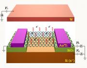
Wu G, Li Z, Tang Z, Wei D, Zhang G, Chen Q, Peng L-M, Wei X.
Silicon Oxide Electron-Emitting Nanodiodes. Advanced Electronic Materials [Internet]. 2018;4:1800136.
访问链接AbstractAbstract Electrically driven on-chip electron sources that do not need to be heated are long pursued, but their realization remains challenging. Here, it is shown that a nanogap formed by two electrodes on a silicon oxide substrate functions as an electron-emitting nanodiode after the silicon oxide in the nanogap is electrically switched to a high-resistance conducting state. A nanodiode based on graphene electrodes can be turned on by a voltage of ≈7 V in ≈100 ns and show an emission current of up to several microamperes, corresponding to an emission density of ≈106 A cm−2 and emission efficiency as high as 16.6%. We attribute the electron emission to be generated from a metal–insulator–metal tunneling diode on the substrate surface formed by the rupture of conducting filaments in silicon oxide. An array of 100 nanodiodes exhibits a global emission density of 5 A cm−2 and stable emission with negligible current degradation over tens of hours under modest vacuum. The combined advantages of a low operating voltage, fast temporal response, high emission density and efficiency, convenient fabrication and integration, and stable emission in modest vacuum make silicon oxide electron-emitting nanodiodes a promising on-chip electron sources.
Tang Z, Han Y, Sun M, Li X, Wu G, Gao S, Chen Q, Peng L-M, Wei X.
Controlling the Growth of Single Nanowires in a Nanowire Forest for Near Infrared Photodetection. ACS Applied Nano Materials [Internet]. 2018:null.
访问链接