Xue Z, Sun M, Dong T, Tang Z, Zhao Y, Wang J, Wei X, Yu L, Chen Q, Xu J, et al. Deterministic Line-Shape Programming of Silicon Nanowires for Extremely Stretchable Springs and Electronics. Nano Letters [Internet]. 2017;17:7638-7646.
访问链接AbstractLine-shape engineering is a key strategy to endow extra stretchability to 1D silicon nanowires (SiNWs) grown with self-assembly processes. We here demonstrate a deterministic line-shape programming of in-plane SiNWs into extremely stretchable springs or arbitrary 2D patterns with the aid of indium droplets that absorb amorphous Si precursor thin film to produce ultralong c-Si NWs along programmed step edges. A reliable and faithful single run growth of c-SiNWs over turning tracks with different local curvatures has been established, while high resolution transmission electron microscopy analysis reveals a high quality monolike crystallinity in the line-shaped engineered SiNW springs. Excitingly, in situ scanning electron microscopy stretching and current–voltage characterizations also demonstrate a superelastic and robust electric transport carried by the SiNW springs even under large stretching of more than 200%. We suggest that this highly reliable line-shape programming approach holds a strong promise to extend the mature c-Si technology into the development of a new generation of high performance biofriendly and stretchable electronics.
Wang Y, Wu G, Xiang L, Xiao M, Li Z, Gao S, Chen Q, Wei X*.
Single-walled carbon nanotube thermionic electron emitters with dense, efficient and reproducible electron emission. Nanoscale [Internet]. 2017;9:17814 - 17820.
访问链接AbstractThermionic electron emitters have recently been scaled down to the microscale using microfabrication technologies and graphene as the filament. While possessing several advantages over field emitters, graphene-based thermionic micro-emitters still exhibit low emission current density and efficiency. Here, we report nanoscale thermionic electron emitters (NTEEs) fabricated using microfabrication technologies and single-walled carbon nanotubes (SWCNTs), the thinnest conducting filament we can use. The SWCNT NTEEs exhibit an emission current density as high as 0.45 × 10⁵ A cm−2, which is superior to that of traditional thermionic emitters and five orders of magnitude higher than that of graphene-based thermionic emitters. The emission characteristics of SWCNT NTEEs are found to strongly depend on the electrical properties of the SWCNTs, with metallic SWCNT NTEEs showing a substantially lower turn-on voltage and more reproducible emission performances than those based on semiconducting SWCNTs. Our results indicate that SWCNT NTEEs are promising for electron source applications
Shu J, Wu G, Gao S, Liu B, Wei X, Chen Q.
Influence of water vapor on the electronic property of MoS2 field effect transistors. Nanotechnology [Internet]. 2017;28(20):204003.
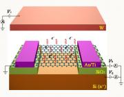
访问链接AbstractThe influence of water vapor on the electronic property of MoS2 field effect transistors (FETs) is studied through controlled experiments. We fabricate supported and suspended FETs on the same piece of MoS2 to figure out the role of SiO2 substrate on the water sensing property of MoS2. The two kinds of devices show similar response to water vapor and to different treatments, such as pumping in the vacuum, annealing at 500 K and current annealing, indicating the substrate does not play an important role in the MoS2 water sensor. Water adsorption is found to decrease the carrier mobility probably through introducing a scattering center on the surface of MoS2. The threshold voltage and subthreshold swing of the FETs do not change obviously after introducing water vapor, indicating there is no obvious doping and trap introducing effects. Long time pumping in a high vacuum and 500 K annealing show negligible effects on removing the water adsorption on the devices. Current annealing at high source-drain bias is found to be able to remove the water adsorption and set the FETs to their initial states. The mechanism is proposed to be through the hot carriers at high bias.
Wei X, Chen Q, Peng L-M.
Thermionic electron emission from single carbon nanostructures and its applications in vacuum nanoelectronics. MRS Bulletin [Internet]. 2017;42(7):493-499 .
访问链接AbstractNanoscale electron sources with high electron-emitting performance are of great interest in vacuum nanoelectronics. Resembling traditional thermionic emission sources based on a hot tungsten filament, a hot carbon nanotube or graphene can function as a nanoscale electron source because of its excellent thermal stability and electrical conductivity. In this article, studies of thermionic emission from single hot carbon nanostructures are overviewed, emphasizing their differences in physics from macroscopic thermionic emission as well as potential applications in vacuum nanoelectronics. Due to their low dimensionality, nanoscale size, and nonequilibrium electron distribution, Richardson’s Law, which governs thermionic emission from macroscopic metals, breaks down in the case of thermionic emission from single carbon nanostructures, and an internal electric field in a carbon nanostructure can contribute directly to its thermionic emission. Graphene-based nanoscale thermionic emission sources, source arrays, and vacuum transistors have been fabricated and demonstrated to exhibit the advantages compared to those based on field emission. The advances imply the promise of realizing high-performance nanoscale electron sources and vacuum electronic devices based on thermionic emission.
Li X, Cheng S, Deng S, Wei X, Zhu J, Chen Q.
Direct Observation of the Layer-byLayer Growth of ZnO Nanopillar by In situ High Resolution Transmission Electron Microscopy. SCIENTIFIC REPORTS [Internet]. 2017;7:40911.
访问链接AbstractCatalyst-free methods are important for the fabrication of pure nanowires (NWs). However, the growth mechanism remains elusive due to the lack of crucial information on the growth dynamics at atomic level. Here, the noncatalytic growth process of ZnO NWs is studied through in situ high resolution transmission electron microscopy. We observe the layer-by-layer growth of ZnO nanopillars along the polar [0001] direction under electron beam irradiation, while no growth is observed along the radial directions, indicating an anisotropic growth mechanism. The source atoms are mainly from the electron beam induced damage of the sample and the growth is assisted by subsequent absorption and then diffusion of atoms along the side surface to the top (0002) surface. The different binding energy on different ZnO surface is the main origin for the anisotropic growth. Additionally, the coalescence of ZnO nanocrystals related to the nucleation stage is uncovered to realize through the rotational motions and recrystallization. Our in situ results provide atomic-level detailed information about the dynamic growth and coalescence processes in the noncatalytic synthesis of ZnO NW and are helpful for understanding the vapor-solid mechanism of catalyst-free NW growth.
Li H, Wang J, Gao S, Chen Q, Peng LM, Liu K, Wei X.
Superlubricity between MoS2 Monolayers. Advanced Materials [Internet]. 2017;29(27):1701474 .
访问链接AbstractThe ultralow friction between atomic layers of hexagonal MoS2, an important solid lubricant and additive of lubricating oil, is thought to be responsible for its excellent lubricating performances. However, the quantitative frictional properties between MoS2 atomic layers have not been directly tested in experiments due to the lack of conventional tools to characterize the frictional properties between 2D atomic layers. Herein, a versatile method for studying the frictional properties between atomic-layered materials is developed by combining the in situ scanning electron microscope technique with a Si nanowire force sensor, and the friction tests on the sliding between atomic-layered materials down to monolayers are reported. The friction tests on the sliding between incommensurate MoS2 monolayers give a friction coefficient of ≈10−4 in the regime of superlubricity. The results provide the first direct experimental evidence for superlubricity between MoS2 atomic layers and open a new route to investigate frictional properties of broad 2D materials.