摘要:
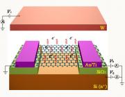
High quality single-crystal CdS nanowire ( NW) networks have been synthesized on Si(111) substrates via the chemical vapour deposition method. X-ray diffraction and selected area electron diffraction show that the NWs in the networks grow along the < 11 (2) over bar0 > directions and their (0001) crystal planes are parallel to the Si(111) substrates. Room-temperature photoluminescence (PL) spectra of single CdS NWs in the networks are dominated by a near-band-edge emission and free from deep-level defect emissions. The PLs resulting from free-exciton and bound-exciton recombinations are detected at 77 K. The results of the electrical transport measurement on the CdS NW networks show that the current can flow through different NWs via the cross-junctions. The resistivity, electron concentration and electron mobility of single NWs in the networks are estimated by fitting the I-V curves measured on single NWs with the metal-semiconductor-metal model suggested by Zhang et al (2006 Appl. Phys. Lett. 88 073102; 2007 Adv. Funct. Mater. at press).
附注:
Ma, R. M. Wei, X. L. Dai, L. Huo, H. B. Qin, G. G.
Website